On July 24, 2026, Samsung Electronics and Broadcom signed a memorandum of understanding worth more than $200 billion, running through 2030, covering next-generation memory, foundry manufacturing, and advanced packaging for AI chips. It’s one of the largest semiconductor partnerships ever disclosed — and it’s built entirely around one category of hardware: AI accelerators.
If you’ve heard the term thrown around but aren’t quite sure what it actually means — or why a single supply deal for them can be worth as much as some countries’ GDP — this is the explainer. We’ll use the Samsung-Broadcom deal as our anchor, then break down what AI accelerators are, why they need such exotic manufacturing, and what this all means for the industry.
First, What Actually Happened in the Deal?
According to Samsung’s own newsroom announcement, the collaboration spans two major fronts: memory and foundry, together valued at over $200 billion across five years. Specifically:
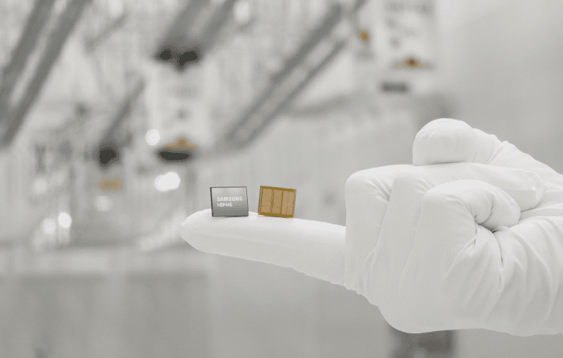
- Memory: Samsung will supply Broadcom with High Bandwidth Memory (HBM), including next-generation HBM4 and HBM4E, purpose-built to feed Broadcom’s AI accelerators.
- Foundry: Broadcom will use Samsung’s 2-nanometer and below manufacturing processes to produce chips, including its Wireless Broadband Communications solutions.
- Packaging: The deal also covers 2.3D and 2.5D advanced packaging, techniques used to physically combine multiple chip components — like compute and memory — into a single, tightly integrated package.
It’s worth flagging, as several industry outlets have noted, that this is a memorandum of understanding rather than a locked-in contract — it represents a strategic intent and estimated scale, not a guaranteed order value. Samsung’s 2nm yields are still being scrutinized, and TSMC’s current dominance in advanced-node manufacturing means the competitive picture won’t shift overnight. Still, the scope and size of the agreement is a real signal of where the industry is placing its bets.
So, What Exactly Is an AI Accelerator?
An AI accelerator is a chip built specifically to handle the kind of math that powers modern AI — mostly matrix multiplication and other operations used in training and running neural networks — far faster and more efficiently than a general-purpose CPU could.
Think of it this way: a CPU is a generalist, good at doing many different kinds of tasks reasonably well, one after another. An AI accelerator is a specialist, built to do one narrow category of math extremely fast, in parallel, across thousands of operations at once. That specialization is exactly why AI accelerators can train and run today’s large language models and image generators at a scale that would be impractical on regular processors.
The Main Types of AI Accelerators
- GPUs (Graphics Processing Units) — originally built for rendering graphics, GPUs turned out to be excellent at the parallel math AI needs too, which is why companies like Nvidia became central to the AI boom.
- Custom AI ASICs (Application-Specific Integrated Circuits) — chips designed from scratch for a specific company’s AI workloads. Google’s TPUs and many of Broadcom’s custom accelerator designs fall into this category. They trade flexibility for efficiency: less general-purpose than a GPU, but often faster and more power-efficient for the exact task they’re built for.
- NPUs (Neural Processing Units) — smaller-scale AI accelerators increasingly built into consumer devices like laptops and phones, handling on-device AI tasks (like camera processing or local assistant features) without needing to reach a data center.
Broadcom, notably, doesn’t sell chips under its own brand the way Nvidia does — it designs custom AI accelerators for large customers (reportedly including major cloud and AI companies) who need chips tailored precisely to their own workloads, and it’s this custom-silicon business that Samsung’s manufacturing capacity is being lined up to support.
Why Manufacturing an AI Accelerator Requires So Much More Than “Making a Chip”
This is where the Samsung deal’s individual pieces — HBM, 2nm, advanced packaging — start to make sense as a set, rather than three separate line items.
Why HBM (High Bandwidth Memory) Matters
AI accelerators are only as fast as the data they can access. A powerful processor sitting idle, waiting for data to arrive, is wasted silicon. High Bandwidth Memory solves this by stacking memory chips vertically and connecting them to the processor with extremely wide, short data pathways — dramatically increasing how much data can move between memory and compute per second, compared to traditional memory layouts.
This is precisely why the memory side of the Samsung-Broadcom deal centers on HBM4 and HBM4E: next-generation AI accelerators are increasingly bottlenecked by memory bandwidth, not just raw processing power, and HBM is currently the industry’s answer to that bottleneck.
Why the Process Node (2nm) Matters
The “2-nanometer” figure refers to the manufacturing process used to etch transistors onto a chip — broadly, a measure of how small and densely packed the transistors can be. Smaller process nodes generally mean more transistors fit in the same physical space, which translates to more processing power and better energy efficiency per chip.
For AI accelerators specifically, this matters enormously: AI data centers are increasingly constrained by power availability and heat, not just chip supply. A more efficient process node means more AI compute per watt — which is a large part of why leading-edge foundry capacity has become one of the most contested resources in the entire tech industry.
Why Advanced Packaging (2.3D/2.5D) Matters
Even with faster memory and a smaller process node, you still need to physically connect the compute chip and the memory chips together efficiently. Advanced packaging techniques like 2.3D and 2.5D integration allow multiple chip components — logic, memory, sometimes networking — to be combined into a single package with much shorter, faster connections than mounting them separately on a circuit board. This is what actually allows an AI accelerator and its HBM stacks to function as a single, fast unit rather than several separate chips talking to each other slowly.
Put together, HBM, advanced nodes, and advanced packaging represent the three biggest engineering bottlenecks in building a modern AI accelerator — which is exactly why a single deal covering all three, at this scale, is considered such a big deal industry-wide.
Why This Deal Matters Beyond Samsung and Broadcom
A few takeaways worth understanding, even if you’re not in the semiconductor business:
- It’s a direct challenge to TSMC’s dominance. TSMC currently manufactures the overwhelming majority of the world’s most advanced AI chips. A $200 billion, multi-year commitment to Samsung’s foundry is a meaningful bet on supply chain diversification — something many AI companies have reportedly wanted, simply to reduce dependence on a single manufacturer.
- It reflects how AI chip deals are being structured differently now. Rather than one-off purchase orders, companies are increasingly locking in long-term, multi-technology partnerships spanning memory, manufacturing, and packaging together — a sign that both sides expect AI infrastructure demand to keep growing for years, not just the next product cycle.
- It underscores how much the “AI boom” is really a hardware story. Every major advance in AI model capability ultimately depends on someone being able to physically manufacture enough of these highly specialized chips — and that manufacturing capacity, not just algorithmic breakthroughs, is increasingly the bottleneck the entire industry is racing to solve.
The Bottom Line
AI accelerators are the actual physical engine behind everything the AI industry talks about — the models, the chatbots, the image generators. What the Samsung-Broadcom deal makes clear is that building these chips has become a full-stack manufacturing challenge, combining next-generation memory, cutting-edge process nodes, and advanced packaging into one enormously expensive, tightly coordinated supply chain. As AI demand keeps climbing, expect more deals like this one — because at this point, the biggest constraint on how much smarter AI gets may not be the algorithms at all. It may simply be how many of these chips the world can actually build.


Share Your Views: